- 您现在的位置:买卖IC网 > Sheet目录490 > NTLUD3A260PZTBG (ON Semiconductor)POWER MOSFET 20V 2A 200 M UDFN6
�� �
�
�NTLUD3A260PZ�
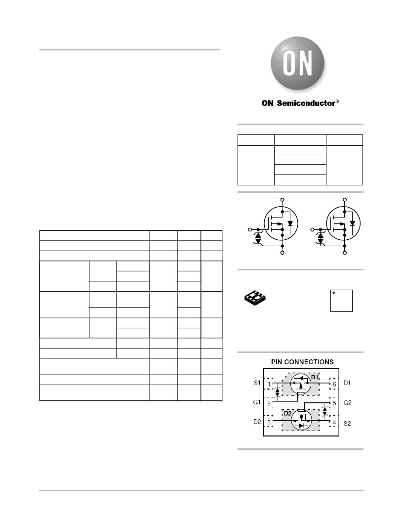
�Power� MOSFET�
�?� 20� V,� ?� 2.1� A,� m� Cool� t� Dual� P� ?� Channel,�
�ESD,� 1.6x1.6x0.55� mm� UDFN� Package�
�Features�
�?� UDFN� Package� with� Exposed� Drain� Pads� for� Excellent� Thermal�
�Conduction�
�?� Low� Profile� UDFN� 1.6x1.6x0.55� mm� for� Board� Space� Saving�
�?� ESD� Protected�
�?� These� Devices� are� Pb� ?� Free,� Halogen� Free/BFR� Free� and� are� RoHS�
�Compliant�
�Applications�
�?� High� Side� Load� Switch�
�?� PA� Switch�
�?� Optimized� for� Power� Management� Applications� for� Portable�
�Products,� such� as� Cell� Phones,� PMP,� DSC,� GPS,� and� others�
�V� (BR)DSS�
�?� 20� V�
�http://onsemi.com�
�MOSFET�
�R� DS(on)� MAX�
�200� m� W� @� ?� 4.5� V�
�290� m� W� @� ?� 2.5� V�
�390� m� W� @� ?� 1.8� V�
�650� m� W� @� ?� 1.5� V�
�D1�
�I� D� MAX�
�?� 2.1� A�
�D2�
�MAXIMUM� RATINGS� (T� J� =� 25� °� C� unless� otherwise� stated)�
�Parameter� Symbol� Value�
�Units�
�G1�
�G2�
�Drain-to-Source� Voltage�
�V� DSS�
�?� 20�
�V�
�Gate-to-Source� Voltage�
�Continuous� Drain� Steady�
�Current� (Note� 1)� State�
�t� ≤� 5s�
�Power� Dissipa-� Steady�
�tion� (Note� 1)� State�
�t� ≤� 5s�
�Continuous� Drain�
�Steady�
�Current� (Note� 2)�
�State�
�T� A� =� 25� °� C�
�T� A� =� 85� °� C�
�T� A� =� 25� °� C�
�T� A� =� 25� °� C�
�T� A� =� 25� °� C�
�T� A� =� 25� °� C�
�T� A� =� 85� °� C�
�V� GS�
�I� D�
�P� D�
�I� D�
�±� 8.0�
�?� 1.7�
�?� 1.2�
�?� 2.1�
�0.8�
�1.3�
�?� 1.3�
�?� 0.9�
�V�
�A�
�W�
�A�
�1�
�6�
�S1� S2�
�P� ?� Channel� MOSFET�
�MARKING�
�DIAGRAM�
�UDFN6� 1�
�CASE� 517AT� AD� M� G�
�m� COOL� t� G�
�AD� =� Specific� Device� Code�
�M� =� Date� Code�
�G� =� Pb� ?� Free� Package�
�Power� Dissipation� (Note� 2)�
�Pulsed� Drain� Current�
�T� A� =� 25� °� C�
�tp� =� 10� m� s�
�P� D�
�I� DM�
�0.5�
�?� 8.0�
�W�
�A�
�(Note:� Microdot� may� be� in� either� location)�
�Operating� Junction� and� Storage�
�Temperature�
�Source� Current� (Body� Diode)� (Note� 2)�
�Lead� Temperature� for� Soldering� Purposes�
�(1/8� ″� from� case� for� 10� s)�
�T� J� ,�
�T� STG�
�I� S�
�T� L�
�-55� to�
�150�
�?� 0.6�
�260�
�°� C�
�A�
�°� C�
�Stresses� exceeding� Maximum� Ratings� may� damage� the� device.� Maximum�
�Ratings� are� stress� ratings� only.� Functional� operation� above� the� Recommended�
�Operating� Conditions� is� not� implied.� Extended� exposure� to� stresses� above� the�
�Recommended� Operating� Conditions� may� affect� device� reliability.�
�1.� Surface� Mounted� on� FR4� Board� using� 1� in� sq� pad� size� (Cu� area� =� 1.127� in� sq�
�[2� oz]� including� traces).�
�2.� Surface-mounted� on� FR4� board� using� the� minimum� recommended� pad� size�
�of� 30� mm� 2� ,� 2� oz.� Cu.�
�(Top� View)�
�ORDERING� INFORMATION�
�See� detailed� ordering� and� shipping� information� in� the� package�
�dimensions� section� on� page� 5� of� this� data� sheet.�
�?� Semiconductor� Components� Industries,� LLC,� 2010�
�September,� 2010� ?� Rev.� 1�
�1�
�Publication� Order� Number:�
�NTLUD3A260PZ/D�
�发布紧急采购,3分钟左右您将得到回复。
相关PDF资料
NTLUF4189NZTAG
MOSFET N-CH 30V 1.2A 6UDFN
NTLUS3192PZTBG
MOSFET P-CH 20V 3.4A SGL 6UDFN
NTLUS3A18PZTBG
MOSFET P-CH 20V 8.2A 6UDFN
NTLUS3A39PZTBG
MOSFET P-CH 20V 5.2A 6UDFN
NTLUS3A40PZTBG
T4 20/8 PCH 2X2 UDFN SING
NTLUS3A90PZTBG
POWER MOSFET 20V 3A 60 MO UDFN6
NTLUS4195PZTBG
MOSFET P-CH 30V 3A SGL 6UDFN
NTMD2C02R2SG
MOSFET N/P-CH COMPL 20V 8-SOIC
相关代理商/技术参数
NTLUD3A50PZ
制造商:ONSEMI 制造商全称:ON Semiconductor 功能描述:a??20 V, a??5.6 A, Cool Dual Pa??Channel, 2.0x2.0x0.55 mm UDFN Package
NTLUD3A50PZTAG
功能描述:MOSFET PFET UDFN 20V 5.6A 50MOHM RoHS:否 制造商:STMicroelectronics 晶体管极性:N-Channel 汲极/源极击穿电压:650 V 闸/源击穿电压:25 V 漏极连续电流:130 A 电阻汲极/源极 RDS(导通):0.014 Ohms 配置:Single 最大工作温度: 安装风格:Through Hole 封装 / 箱体:Max247 封装:Tube
NTLUD3A50PZTBG
制造商:ON Semiconductor 功能描述:PFET UDFN 20V 5.6A 50MOHM - Tape and Reel 制造商:ON Semiconductor 功能描述:REEL / PFET UDFN 20V 5.6A 50MOHM
NTLUF4189NZ
制造商:ONSEMI 制造商全称:ON Semiconductor 功能描述:Power MOSFET and Schottky Diode 30 V, N−Channel with 0.5 A Schottky Barrier Diode, 1.6 x 1.6 x 0.55 mm Cool Package
NTLUF4189NZTAG
功能描述:MOSFET NFET WDFN6 30V 1.5A 200mOhm RoHS:否 制造商:STMicroelectronics 晶体管极性:N-Channel 汲极/源极击穿电压:650 V 闸/源击穿电压:25 V 漏极连续电流:130 A 电阻汲极/源极 RDS(导通):0.014 Ohms 配置:Single 最大工作温度: 安装风格:Through Hole 封装 / 箱体:Max247 封装:Tube
NTLUF4189NZTBG
功能描述:MOSFET NFET WDFN6 30V 1.5A 200mOhm RoHS:否 制造商:STMicroelectronics 晶体管极性:N-Channel 汲极/源极击穿电压:650 V 闸/源击穿电压:25 V 漏极连续电流:130 A 电阻汲极/源极 RDS(导通):0.014 Ohms 配置:Single 最大工作温度: 安装风格:Through Hole 封装 / 箱体:Max247 封装:Tube
NTLUS3192PZ
制造商:ONSEMI 制造商全称:ON Semiconductor 功能描述:Power MOSFET −20 V, −4.2 A, Cool Single P−Channel, ESD, 1.6x1.6x0.55 mm UDFN Package
NTLUS3192PZTAG
功能描述:MOSFET PFET WDFN6 20V 3.4A 85 mOhm RoHS:否 制造商:STMicroelectronics 晶体管极性:N-Channel 汲极/源极击穿电压:650 V 闸/源击穿电压:25 V 漏极连续电流:130 A 电阻汲极/源极 RDS(导通):0.014 Ohms 配置:Single 最大工作温度: 安装风格:Through Hole 封装 / 箱体:Max247 封装:Tube